

The AI Hardware Primer
Everyone is watching the models. The constraint is somewhere else.


Nvidia is down. The frontier labs are heading toward public markets at eye-watering valuations. A Chinese AI lab just released a model that rivals the best American ones at a fraction of the cost. If you’re trying to make sense of what’s happening - and what it means for where to put capital - most of what you’ve read hasn’t explained the part that actually matters. This post does.
Start with what everyone is looking at.
Nvidia stock has sold off. The explanation circulating: AI models are getting more efficient, which means less demand for chips, which means less revenue for Nvidia. Meanwhile Anthropic and OpenAI are reportedly preparing for public markets at valuations in the hundreds of billions. And Kimi K3 - a Chinese AI model released last week - just demonstrated that a non-American lab can match the best frontier models, openly, at a fraction of the cost.
Those three facts feel like they tell a coherent story. Cheaper AI, less hardware demand, American AI companies racing to go public before the window closes. Sell the chips, maybe buy the labs before they list.
That story has a problem. It’s built on a misunderstanding of where the constraint in this buildout actually lives. And the misunderstanding starts with something almost no coverage of the AI trade bothers to explain: what the hardware actually does, and why certain parts of it cannot be made cheaper by software improvements.
The AI buildout runs on a stack - a set of layers, each one resting on the one beneath it. The application you use sits at the top. The materials required to build the whole thing sit at the bottom. Each layer has its own constraints, its own suppliers, its own timelines. What’s happening at the top - models getting cheaper, labs going public - is real. It’s just not the whole picture. The diagram below maps the full stack. Everything in this publication fits somewhere on this diagram. If you understand the diagram, you understand how the rest of the series connects.
Start at the bottom and work up.
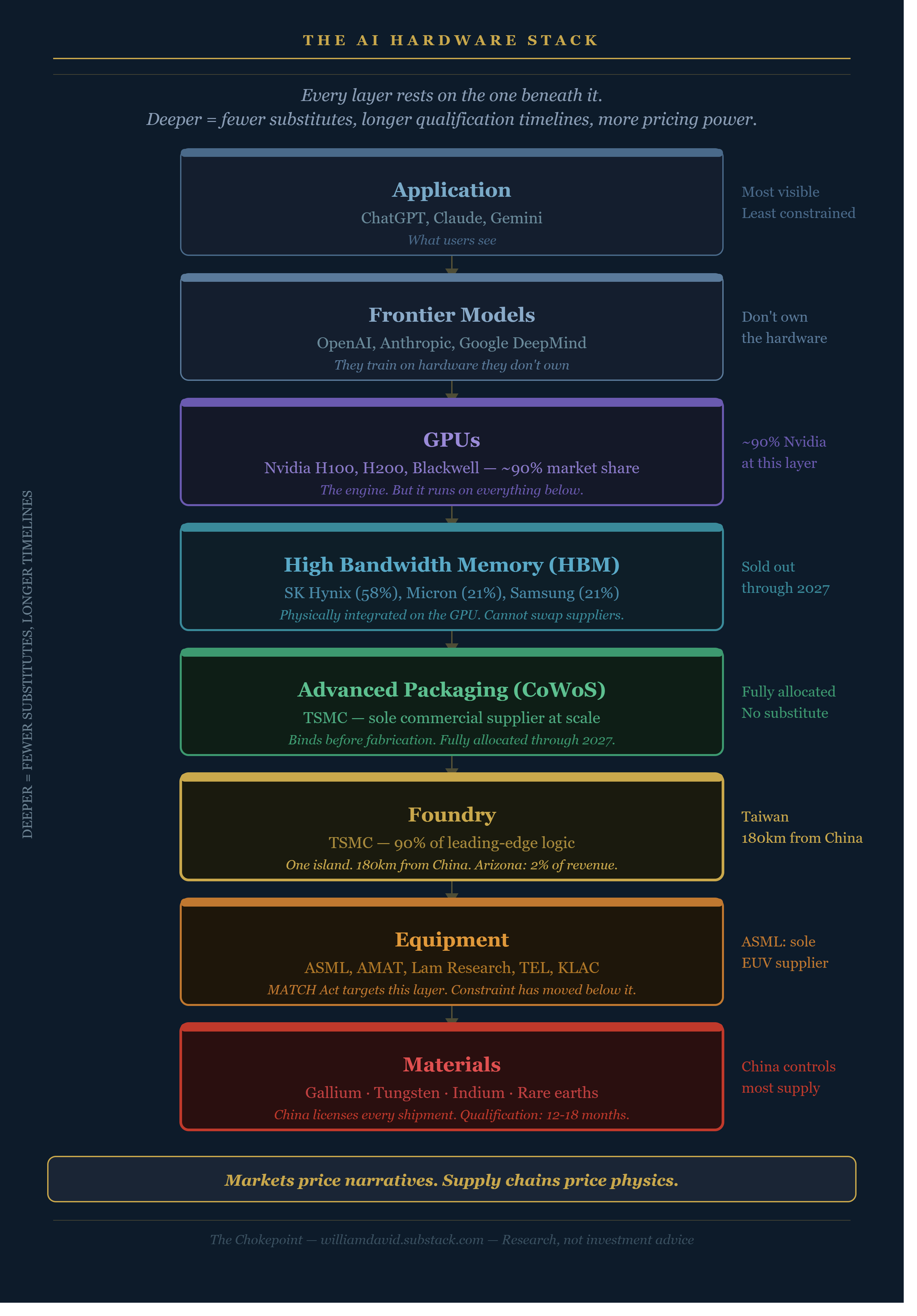
What a chip actually is
A semiconductor chip is a piece of silicon covered in billions of tiny switches. Silicon is useful because it can be made to conduct or resist electricity depending on conditions - that controllable property is what makes computation possible. Those switches - transistors - turn on and off billions of times per second. That switching is computation. Everything an AI model does, every word it generates, every question it answers, is the product of those switches firing in sequence.
The switches have to be impossibly small. The most advanced chips today are built at dimensions measured in nanometers - billionths of a meter. A human hair is roughly 80,000 nanometers wide. The transistors in a leading-edge chip are a few nanometers across. Building them requires machines of almost incomprehensible precision, chemicals of extraordinary purity, and process knowledge accumulated over decades. There is no shortcut. You cannot will a chip fabrication facility into existence with capital alone. The knowledge has to be built, qualified, and proven - and that takes years regardless of how much money goes in.
Why AI runs on a specific kind of chip
Not all chips are the same. The processor in your laptop - a CPU - is optimized for sequential tasks. It does one complex thing after another, very quickly. A GPU was originally designed for graphics rendering, which requires doing millions of simple calculations simultaneously rather than one complex calculation at a time.
AI training and inference happen to require exactly that: massive parallel computation. The GPU became the engine of the AI buildout almost by accident. Nvidia happened to be building the best ones, and its software platform created a switching cost that competitors have spent years trying to overcome.
When a company announces it is spending billions on AI infrastructure, most of that money is going toward clusters of GPUs. Nvidia’s chips - each costing $25,000 to $40,000 - are the workhorses of the buildout. A single large AI training run might use tens of thousands of them simultaneously.
Why one company in Taiwan makes most of them
Here is the fact that most AI coverage buries or ignores entirely: Nvidia does not manufacture its own chips. Neither does AMD, Apple, Google, or most of the companies designing cutting-edge silicon. They design the blueprint and send it to a foundry - a specialized manufacturer that does nothing but fabricate chips.
Taiwan Semiconductor Manufacturing Company is that foundry. TSMC manufactures approximately 90% of the world’s most advanced chips. The GPU powering most AI infrastructure today was designed by Nvidia and built by TSMC. The next generation will be too. There is no meaningful alternative at the leading edge.
TSMC sits on an island 180 kilometers from the Chinese coast. Its most advanced manufacturing capacity - the facilities that can build the chips AI requires - is concentrated in Taiwan. Billions are being committed to build new facilities in Arizona. Arizona is also approximately 2% of TSMC’s current revenue, and its most advanced facilities won’t reach production until 2028 at the earliest.
The constraint isn’t just where TSMC is located. It’s what TSMC does that nobody else can replicate at scale - and the years it takes to qualify any alternative.
Why a chip needs more than fabrication
A chip doesn’t go straight from the fabrication facility to a data center. It has to be packaged - physically connected to memory, power delivery, and other chips in a way that lets them communicate fast enough to be useful.
This is the part of the AI buildout that receives almost no coverage, and it is where some of the most important constraints live.
CoWoS is TSMC’s advanced packaging process. It physically integrates high-bandwidth memory with a GPU on the same silicon platform - a thin layer that allows the two to communicate at speeds a conventional circuit board cannot match. Without this integration, the most powerful AI chips cannot function at their rated performance. The memory and the processor need to be that close to each other, physically, for the data transfer speeds that AI inference requires.
TSMC is the only commercial supplier of this packaging at scale. It is fully allocated through 2027. When TSMC’s CEO said on the most recent earnings call that packaging capacity is “so tight it is limiting my customers’ growth,” he was describing a physical constraint that no amount of capital can quickly resolve. You can announce a new facility. You cannot qualify one in a quarter.
The memory the chip depends on
The memory that sits alongside the GPU in that package is not the same memory as in your laptop. Regular memory is fast enough for most computing tasks. AI inference at scale requires something faster - memory that can transfer data to the processor almost instantaneously, in massive volumes, without lag.
High Bandwidth Memory - HBM - stacks multiple memory chips vertically, connects them through microscopic channels, and places them directly beside the GPU. It is physically inseparable from the chip it serves. Three companies make it at commercial scale: SK Hynix, Micron, and Samsung. SK Hynix holds approximately 58% of the market.
Here is the detail that matters most: switching HBM suppliers requires redesigning the entire chip package from scratch. The memory and the GPU are co-designed. A chip built around one manufacturer’s HBM cannot simply swap in another’s without an 18-month redesign cycle minimum. That is not a commercial negotiating position. That is a physical constraint.
This is the layer the Semiconductor & AI Hardware Series spends the most time on. If you want the full argument - why the shortage persists through 2027, why the switching cost is structural, and what the investment implications are - that series is where it lives.
What a model actually needs to run
This is where everything above connects to the news that sent Nvidia lower and left many investors confused.
When an AI model generates a response, it draws on everything it learned during training. That accumulated knowledge is stored as numbers - billions or trillions of them - called weights. They encode, statistically, how language works: what words follow other words, how concepts relate, what a coherent answer looks like. Every response the model generates is the product of those weights doing work.
All of those weights have to be loaded into HBM and kept there the entire time the model is running. The model cannot predict which weights it will need next, so all of them have to be within reach at all times.
Think of it like a chef. A great chef needs two things: the skill to cook, and the ingredients within reach. Compute is the cooking. The weights in memory are everything on the counter.
You can make the chef faster. You cannot make a meal with ingredients that aren’t there.
What Kimi K3 actually showed
The important point isn’t the architecture itself. It’s that software efficiency and hardware requirements are not the same thing.
Kimi K3 uses an architecture called Mixture of Experts. Instead of activating all 2.8 trillion weights for every response, the model routes each piece of a question to a specialized subset - roughly 50 billion weights at a time. Less active computation per response. A more efficient model.
The market drew a conclusion: models are getting more efficient, chip demand will fall.
Here is what the market missed. All 2.8 trillion weights still have to be on the counter. Kimi K3 requires several terabytes of HBM to exist in a runnable state - regardless of how efficient each individual response is. When Kimi K3 paused new subscriptions 48 hours after launch because demand overwhelmed capacity, it was not a compute problem. It was a memory problem. The model needed more HBM than it had available.
More efficient model. Same memory requirement. Different hardware. Different constraint.
The efficiency argument compresses the compute bill. It does not compress the memory bill. Those are different chips, different supply chains, and they are not moving in the same direction.
Why the frontier labs aren’t where the constraint lives
Which brings us to Anthropic, OpenAI, and what to make of these companies when they eventually reach public markets.
The frontier labs have built the most capable AI systems in the world and are genuinely changing how businesses work. They are also sitting on top of a supply chain they don’t control.
OpenAI trains on TSMC chips. Anthropic runs inference on servers full of HBM. Neither manufactures the hardware. Neither controls the materials. If CoWoS packaging capacity tightens - and it has - they pay more and wait longer. If HBM is allocated to Nvidia first - and it is - they buy what’s left. Their compute bills are enormous. The hardware that determines how much they can grow and what it costs is controlled by companies they have no ownership in.
The frontier labs are the most visible part of the AI buildout. They are not the most constrained part. The most constrained parts - the fabrication layer, the packaging layer, the memory layer - tend to have more durable pricing power than the application layer above them.
This is not an argument against the frontier labs. It is an argument for understanding where in the stack the constraint actually lives. The market spends most of its time pricing what’s visible. The more durable question is what makes the visible part possible.
The layer underneath everything
One more thing.
Every layer described above depends on materials that are difficult to produce, geographically concentrated, and in several cases controlled by China through export licensing. Tungsten is in the contacts of every memory chip. Gallium - under Chinese export control - goes into the power electronics that run data centers. Indium phosphide is at the heart of the optical connections that move data between chips at the speeds AI infrastructure requires.
The semiconductor story and the critical minerals story are the same argument at different layers of the same stack. The chip constraint is real. The constraint underneath the chip is also real. And the further down the stack you go, the fewer substitutes exist and the longer the timelines become before anything changes. That argument runs through the Critical Minerals Series at the full archive.
What to do with this
This post is not a recommendation. It is a map.
The AI buildout is the largest capital deployment in modern industrial history. Most coverage focuses on which model is winning, which lab is ahead, which application is growing fastest. Those are real questions. They are not the only questions.
The questions that tend to matter more over time: where does the constraint live? Who controls the layer that everything above it depends on? What would have to be true for that constraint to resolve - and how long would that take?
Next time you read that AI is getting cheaper, ask which layer is getting cheaper. The model layer might be. The memory layer isn’t. The packaging layer isn’t. The materials layer isn’t.
Those are different parts of the same buildout. They are not all going in the same direction.
The Semiconductor & AI Hardware Series and the Critical Minerals Series explore each of these layers in depth.
Ready to go deeper? The Semiconductor & AI Hardware Series starts here:
Semiconductors & AI Hardware, Part 1: The Compute Layer

The AI industry is spending $700 billion this year on infrastructure it cannot build without China. Not because it chose the dependency. Because the physical reality of what an AI chip requires runs through supply chains China controls at every layer simultaneously - and on July 1, one of those layers went into an unconfirmed halt.
The full archive is at williamdavid.substack.com.
This post is for informational purposes only and is not investment advice. The Chokepoint is an independent investment research publication. Nothing in this publication should be construed as a recommendation to buy, sell, or hold any security. All company references are provided for informational and contextual purposes only. Conduct independent due diligence and consult a qualified financial advisor before making any investment decisions.